


QRコード

お問い合わせ


ファックス
+86-579-87223657


住所
中国浙江省金華市武夷県紫陽街Wangda Road


Vetek Semiconductorは、半導体業界向けの多孔質SICセラミックの大手メーカーです。 ISO9001に合格したVetek Semiconductorは、品質を十分に制御できます。 Vetek Semiconductorは、常に多孔質SICセラミック産業の革新者およびリーダーになることに取り組んできました。

多孔質SICセラミックディスク
多孔質SICセラミックは、高温で発射され、多数の相互接続または閉じた細孔があるセラミック材料です。また、2〜100umの範囲の細孔サイズを備えた微孔性真空吸引カップとしても知られています。
多孔質SICセラミックは、冶金、化学産業、環境保護、生物学、半導体およびその他の分野で広く使用されています。多孔質SICセラミックは、発泡法、ゾルゲル法、テープ鋳造法、固体焼結方法、含浸熱分解法によって調製できます。

焼結方法による多孔質SICセラミックの調製
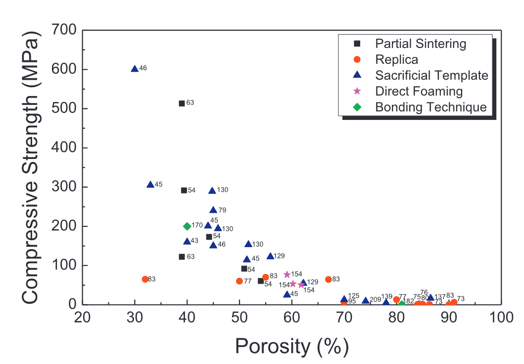
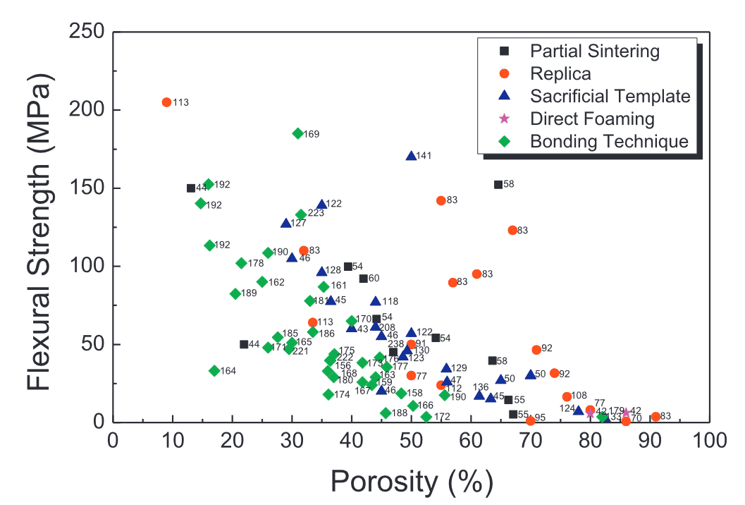
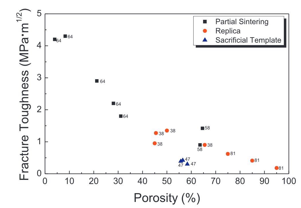
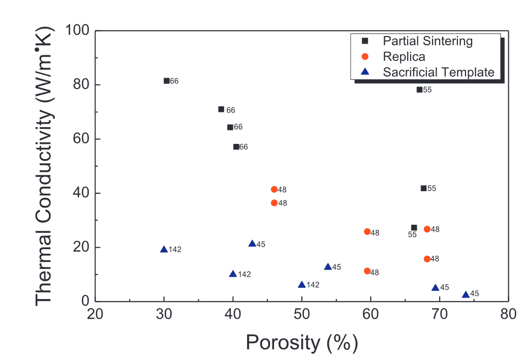
多孔性の関数としてさまざまな方法で調製された多孔質炭化物セラミックの特性

半導体ウェーハ製造における多孔質SICセラミックス吸引カップ
Vetek半導体の多孔質SICセラミックは、半導体生産におけるクランプと運搬の役割を果たします。それらは密で均一で、強度が高く、空気透過性が良好で、吸着が均一です。
彼らは、ウェーハのインデントやチップの静電破壊などの多くの困難な問題に効果的に対処し、非常に高品質のウェーハの処理を達成するのに役立ちます。
多孔質SICセラミックの作業図:

多孔質SICセラミックの動作原理:シリコンウェーハは、真空吸着原理によって固定されています。加工中、多孔質SICセラミックの小さな穴を使用して、シリコンウェーハとセラミック表面の間に空気を抽出するため、シリコンウェーハとセラミック表面が低圧になり、シリコンウェーハが固定されます。
処理後、プラズマ水は穴から流れ出て、シリコンウェーハがセラミック表面に付着するのを防ぎ、同時にシリコンウェーハとセラミック表面がきれいになります。

多孔質SICセラミックの微細構造
強調の利点と機能:
●高温抵抗
●摩耗に対する抵抗
●耐薬品性
●機械的強度が高い
●再生しやすい
●優れた熱衝撃耐性
アイテム
ユニット
多孔質SICセラミック
孔径
1つ
10〜30
密度
g / cm3
1.2〜1.3
表面ルグHNESS
1つ
2.5〜3
空気吸収値
KPA
-45
曲げ強度
MPA
30 誘電率
1MHz
33 熱伝導率
w/(m・k)
60〜70
多孔質SICセラミックにはいくつかの高い要件があります:
1。強い真空吸着
2。フラットネスは非常に重要です。そうしないと、操作中に問題が発生します
3.変形も金属不純物もありません
したがって、Vetek半導体の多孔質SICセラミックの空気吸収値は-45kpaに達します。同時に、彼らは工場を出るために不純物を除去する前に1200℃で1.5時間和らげられ、真空バッグに包装されます。
多孔質SICセラミックは、ウェーハ処理技術、転送、その他のリンクで広く使用されています。彼らは、結合、ダイシング、取り付け、研磨、およびその他のリンクに大きな成果を上げてきました。


Order precision-engineered Porous SiC ceramics from Veteksemicon—ideal for thermal uniformity and gas control in semiconductor systems.
Veteksemicon’s porous silicon carbide (SiC) components are engineered for high-temperature plasma processes and advanced gas flow control. Ideal for PECVD, ALD, vacuum chucks, and gas distribution plates (showerheads), these components offer excellent thermal conductivity, thermal shock resistance, and chemical stability.
Our porous SiC features a controlled pore structure for consistent gas permeability and uniform temperature distribution, reducing defect rates and enhancing yield. It is widely used in wafer handling platforms, temperature equalizing plates, and vacuum holding systems. The material ensures mechanical durability under corrosive and high-load thermal conditions.
Contact Veteksemicon today to request custom Porous SiC solutions or detailed engineering parameters.
+86-579-87223657
中国浙江省金華市武夷県紫陽街Wangda Road